Circuit diagram:
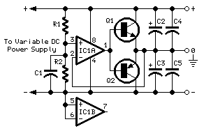
Parts:
R1,R2____________4K7 1/2W 1% or 2% Metal Oxide Resistors


C1,C4,C5_______100nF  63V Polyester Capacitors
C2,C3__________220µF  25V Electrolytic Capacitors

Q1____________BD437   45V 4A NPN Transistor
Q2____________BD438   45V 4A PNP Transistor

IC1___________LM358   Low Power Dual Op-amp

Input and output connecting terminals etc.
Comments:
This design was conceived as an add-on for the Variable DC Power Supply, a very successful circuit posted to this website in the year 2000.
This simple unit provides a dual-rail variable output ranging from ±2.5V to ±15Vdc with precise tracking of the positive and negative output voltages, still retaining the current limiting and short-proof capabilities of the "master" circuit.
As the purpose of such a dual-rail design is to supply experimental or under-repair circuits, the maximum current output delivered was deliberately kept to about 500 - 600mA per rail, thus avoiding the use of expensive power transistors and complex circuitry.
Notes:
- The circuit can be placed into the existing Variable DC Power Supply metal cabinet.
- Q1 and Q2 must be mounted on heatsinks. Usually, bolting them to the metal case (through insulating washers etc.) proved effective.
- The full ±15V output can be achieved only if the secondary winding of the supply Transformer used in the Variable DC Power Supply is rated at 48V minimum (center tapped).
- When using this circuit, please set the Current-limit control (P1) of the Variable DC Power Supply to any value comprised in the 50mA - 1A range but not higher.
- The second Op-amp (IC1B) contained in the LM358 chip was not used, but its input pins were tied to the negative supply and the output was left open.